Understanding And Designing Guitar Effects Pedals
A Beginners Guide
Dissecting the MXR Distortion+
Now we're getting somewhere. We have some understanding of how components are used to achieve particular functions, and we should probably illustrate this in a real example. The MXR Distortion+ is a distortion pedal (shock), and is quite a neat example of all we've learned so far.
It's not completely necessary to understand how a distortion effect works at this stage, as we're mostly interested in the function of each of the components here, rather than what the pedal is actually doing. However, we will cover how distortion works in a separate page later on.
The MXR Distortion+
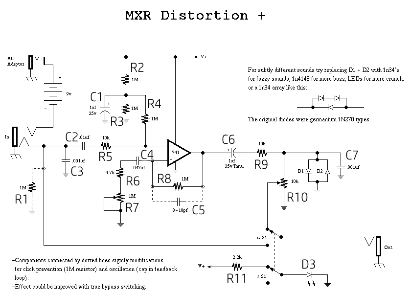
This version of the circuit includes some modifications (indicated with dotted connections), and doesn't include true-bypass switching.
R1 is a pull down resistor. In the image, the effect is in it's on state (see the switch at the bottom right of the image). When the circuit is switched off, the input signal goes straight to the output (as this isn't a true bypass circuit, some of the signal will also make it's way into the effect). Whilst bypassed, capacitor C2 will begin to charge up on the outboard side due to the leakage current pushed through by the biasing voltage. Resistor R1 provides a path to ground for the leakage current to prevent it from charging C2. R1 is also large enough that it won't significantly affect the signal when the effect is on.
R2 and R3 form a potential divider, and create a DC bias voltage. This DC voltage is used to 'shift' the center of our input signal away from \(0V\), and up to \(4.5V\), allowing it to take advantage of the full range of the op-amp's output.
C2 is a coupling capacitor. It blocks the DC current from the power supply from flowing back into the source (our guitar circuitry). Without this capacitor, the DC biasing would not be properly achieved.
C1 is a power supply smoothing capacitor, and is required because this is a real circuit, connected to a real power supply. As we'll see when we make our own overdrive pedal, this capacitor isn't so necessary when using a \(9V\) battery as our supply, because they produce a 'cleaner' voltage that doesn't fluctuate so much. However, this schematic also has the option of using a wall-wart supply, and this power supply is likely to be much noisier and less constant - this is where the capacitor is really doing its duty.
R4 is a slightly complicated one. We wouldn't need R4 if we didn't have C1, but to smooth variations in the power supply, C1 is an important component. But now the combination of C1 and R3 in parallel is important. The reactance of C1 to a \(1kHz\) signal is about \({1 \over 2 \times \pi \times f \times C}=160\Omega\). In parallel with the \(1M\Omega\) resistor, the effective resistance of the pair is still about \(160\Omega\). If R4 wasn't there, our signal would have a low resistance path to ground through this pair. By adding a high resistance to this path of \(1M\Omega\) (R4), we can prevent the signal from bleeding to ground, and maintain it's strength at the non-inverting input of the op-amp.
R5 is a current limiting resistor, that will protect the sensetive operational amplifier from electro-static discharge (ESD). If the guitar lead is plugged in to the pedal but is left disconnected at the other end, a static charge could build up on the plug ...
C3 forms a low-pass filter in combination with the source impedance. This acts to reduce high frequency noise on the input.
R6, R7, and R8 define the gain of this non-inverting op-amp configuration.
C4 keeps the inverting input centred around the 4.5V bias. Without it, the DC bias would be amplified too, so the supply rails would end up clipping our signal.
C6 removes our DC bias from the output signal, so the pedal output is centred around \(0V\), like the input.
D1 and D2 clip the signal to produce the 'overdrive' effect. This way, we don't have to push any of our components to their limits and risk damaging them. We'll look at clipping in our section on distortion, and we'll see how diodes clip a signal in this configuration and others when we get to building our own basic overdrive pedal.
R9 limits the current through the diodes (and seems to make the response symmetric?)
C7 is a filter to remove high frequency noise from the output.
R10 controls the volume by effectively creating a voltage divider. The output is measured between the wiper and the bottom pin of the potentiometer (effectively the bottom resistor in the voltage divider created by a potentiometer). As the wiper moves down, the resistance between the top and middle pins increases, whilst the opposite is true for the bottom resistor. This means more voltage is being dropped across the 'top' part of the potentiometer, and less across the bottom (where we are measuring our output). A smaller voltage across our output then means that the signal out of the pedal is quieter.
D3 is an 'on' indicator LED, and quite simply, it tells you when the pedal is on... Easy. As the pedal is switched on, the circuit is closed and current can flow from power to ground via the LED, illuminating it.
R11 is a current limiting resistor to protect D3, the indicator LED. Diodes are semiconductors and don't take well to spikes in current. This resistor limits the current flow through the LED so we don't accidentally burn it out.